Parameter Test Solution

Dynamic Test Solution AVATAR-D
1. Dynamic test solution for SiC MOSFET based on AVATAR-D-NW platform - Low-sensitivity technology
(1)Based on the AVATAR-D-NW mass production testing machine platform, achieved low inductance of 13.7nH with good waveform quality.
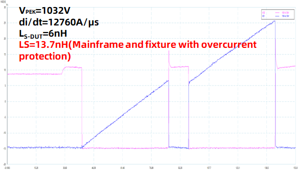
Low-inductance DIB measured waveform
Test Plan:VDS=780V、ID1=660A,ID2=1320A,VGS=15V/-4V
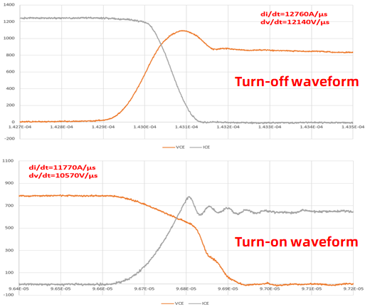
(2)Based on the AVATAR-D-II mass production testing machine platform, the HPD device achieved a low inductance of 22-26nH and good waveform quality.
HPD SiC MOSFET:
- ID =450A, VDS= 400V, VGS = 15V/-4V, RG(ON) = 2.4Ω, RG(OFF) = 5.1Ω
- Parasitic inductance 22~26nH, unit-to-unit difference ±2nH
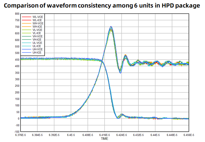
The consistency among the 6 units is good, with waveforms largely overlapping.
HPD SiC MOSFET:
- ID =450A, VDS= 400V, VGS = 15V/-4V, RG(ON) = 2.4Ω, RG(OFF) = 5.1Ω
- Parasitic inductance 22~26nH, unit-to-unit difference ±2nH
The consistency among the 6 units is good, with waveforms largely overlapping.

2. Dynamic test solution for SiC MOSFET based on AVATAR-D-NW platform - Low-sensitivity technology
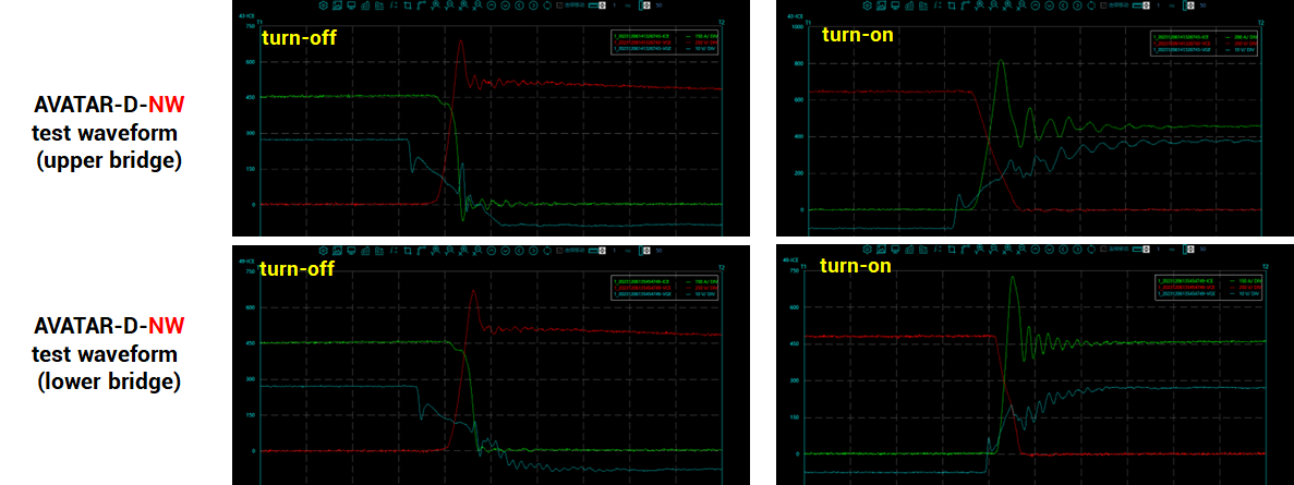
(1)The AVATAR-D-NW host and fixture have been further optimized, the parasitic inductance has been further reduced, and the waveform quality has been further improved.
Average stray inductance is around 14nH (excluding device parasitic inductance)
Stray inductance deviation between bridge arms is less than 1nH
Stray inductance deviation between upper and lower bridges is less than 3nH
Average stray inductance is around 14nH (excluding device parasitic inductance)
Stray inductance deviation between bridge arms is less than 1nH
Stray inductance deviation between upper and lower bridges is less than 3nH
(2) The waveforms of the upper and lower bridge arms measured by the AVATAR-D-NW platform have very small differences.
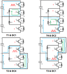
- 3. Photovoltaic-Related Three-Level Topology Module Testing Solution
Type I three-level Double-pulse Test Example:
- 4. Auxiliary Functions of the AVATAR-D/S-NW Platform: Vacuum Drawing, High - Pressure Nitrogen Filling, and Temperature Control (-55℃~200℃)Vacuum drawing: Prevents oxidation, used for DBC, AMB, KGD testing.
High - pressure nitrogen filling: Prevents arcing/oxidation, used for high - voltage or SiC - related DBC, AMB, KGD testing.
Temperature control: Used for characterizing the temperature properties of various devices.